Advanced R&D Division

Engineering the
hardest problems
in hardware.

From multilayer PCB design to sub-8 GHz RF systems — we tackle complexity at every layer of the stack, with world-class instruments and the engineering discipline to back it up.
See the four disciplinesTalk to an RF engineer
8 GHz
RF range
16-layer
PCB capability
100%
DFM reviewed
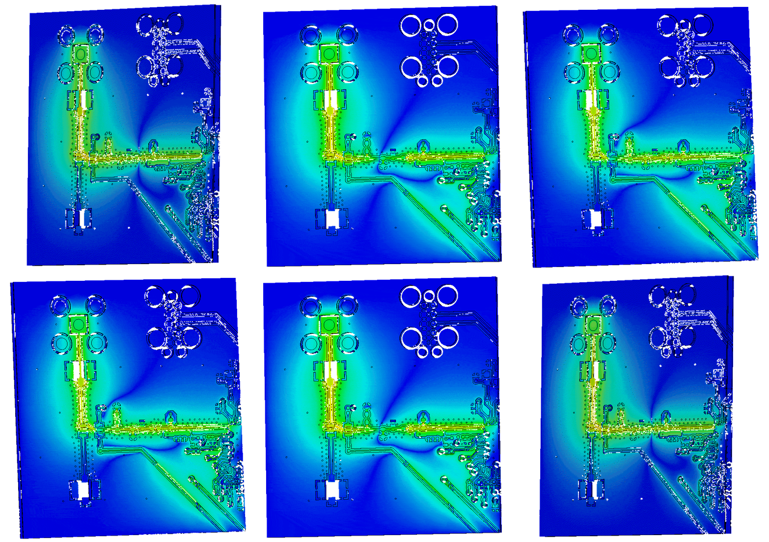
CST Studio electromagnetic field simulation

Core Expertise

Four disciplines. One integrated lab.

Hardware

PCB Design

Advanced multilayer board design for the most demanding applications. From HDI stack-ups to high-speed differential pairs, every layout is engineered for signal integrity, thermal performance, and DFM compliance from day one.

  • Up to 16-layer HDI with blind/buried vias
  • Impedance-controlled routing & SI simulation
  • High-speed design: DDR5, PCIe 5.0, USB 4.0
  • Thermal management & power delivery networks
  • IPC-2221 / IPC-6012 design rules, full DFM review
RF / Microwave

Advanced RF Engineering

End-to-end RF and microwave design from antenna conception to certification readiness. Our shielded lab supports characterization from 100 MHz to 8 GHz, with in-house EMC pre-compliance to eliminate costly surprises at the certification lab.

  • RF/microwave circuit design to 8 GHz
  • Custom antenna design and pattern measurement
  • EMC/EMI pre-compliance and mitigation
  • High-frequency transmission line engineering
  • Certification support: FCC, CE, IC, RED
Sourcing

Component Selection

Intelligent BOM engineering that balances performance, availability, and cost across the full product lifecycle. We identify obsolescence risks early and build in second-source options so your supply chain never becomes a design constraint.

  • Performance-optimized component selection
  • Lifecycle & obsolescence risk management
  • Multi-source and pin-compatible alternatives
  • Supply chain qualification & vendor evaluation
  • Full BOM traceability and documentation
Efficiency

Cost Optimization

Design-for-cost methodology embedded from the architecture phase, not bolted on at the end. We reduce BOM complexity, identify commodity substitutions, and support supplier negotiations to hit target margins without compromising reliability.

  • Design-for-cost analysis at schematic stage
  • BOM consolidation and part count reduction
  • Commodity substitution without compromising spec
  • Supplier negotiation support and volume breaks
  • Total cost-of-ownership modeling

Lab Equipment

Latest-generation instruments.
No compromises.

Our lab is equipped with current-generation test and measurement platforms from the most trusted names in the industry, alongside the latest development kits for rapid wireless prototyping. Every instrument is regularly calibrated and traceable to national measurement standards.


RF & Signal Analysis
Rohde & Schwarz
Instruments
  • Spectrum Analyzer — 1 Hz to 26.5 GHz
  • Vector Network Analyzer — 100 kHz to 20 GHz
  • Signal Generator — DC to 6 GHz, modulation-capable
  • Real-Time Oscilloscope — 16 GHz, 80 GSa/s
  • EMI Test Receiver — CISPR-compliant
Test & Measurement
Tektronix
Instruments
  • Mixed Domain Oscilloscope — 1 GHz, 5 GSa/s
  • Arbitrary Function Generator — 100 MHz
  • Digital Multimeter — 6.5 digit precision
  • Protocol Analyzer — USB, PCIe, DDR
  • Power Analyzer — DC to 2 MHz bandwidth
Power Profiling & Analysis
Qoitech
Instruments
  • Otii Ace Pro — power profiler & source measure unit
  • Programmable isolated supply — 0 to 25 V
  • Current measurement — 0.4 nA resolution, up to 5 A
  • Sampling rate — up to 50 kSa/s
  • Battery & energy optimization for embedded/IoT
Wireless SoC & Rapid Prototyping

Modern Development Kits

Instruments
  • Nordic nRF — Bluetooth LE, Thread & Matter SoCs
  • Espressif — Wi-Fi / BLE SoC dev boards
  • Qorvo — UWB & ultra-low-power wireless kits
  • InPlay — connectionless BLE beacon platforms
  • e-peas — energy-harvesting PMIC evaluation kits
  • Silicon Labs — multiprotocol wireless dev kits

All instruments are regularly calibrated and NIST-traceable. EMC pre-compliance measurements align with CISPR 11/22 and FCC Part 15 methodology.

Software & Tools

Professional-grade tools.
Simulation before silicon.

PCB Design & Layout

Altium Designer

Altium Designer

Industry-leading EDA platform for complete PCB design, from schematic capture through layout, design rule checking, and manufacturing output generation.

  • Full schematic capture with hierarchical design
  • Advanced layout with constraint-driven routing
  • Real-time DRC and signal integrity analysis
  • Full manufacturing output: Gerber, ODB++, IPC-2581
  • Component library management and supplier integration
3D EM Simulation

CST Studio Suite

CST Studio Suite

State-of-the-art 3D electromagnetic simulation for RF, antenna, and signal integrity analysis. Enables full-wave solver-level verification before any physical prototype.

  • Full-wave 3D EM simulation (FIT, FEM, MoM)
  • Antenna design, optimization, and pattern synthesis
  • Signal integrity: channel modeling, eye diagrams
  • EMC/EMI field simulation and shielding analysis
  • Co-simulation with circuit and system-level tools

Manufacturing Partners

From prototype to production.
Trusted fabrication partners.

We work hand-in-hand with established PCB fabrication and assembly houses and IoT hardware manufacturers to carry every design from first prototype through volume production — without compromising on quality, lead time, or cost.


Accent Systems
JLCPCB
PCBWay
Start a conversation

Bring us your
hardest hardware challenge.

Whether you're fighting signal integrity on a high-speed bus, chasing an elusive RF emission, or need a BOM that survives a supply chain shock — the lab is ready.

Discuss your project